Nvidia ‘likely the most concerned’ as Huawei bets on new chip architecture law
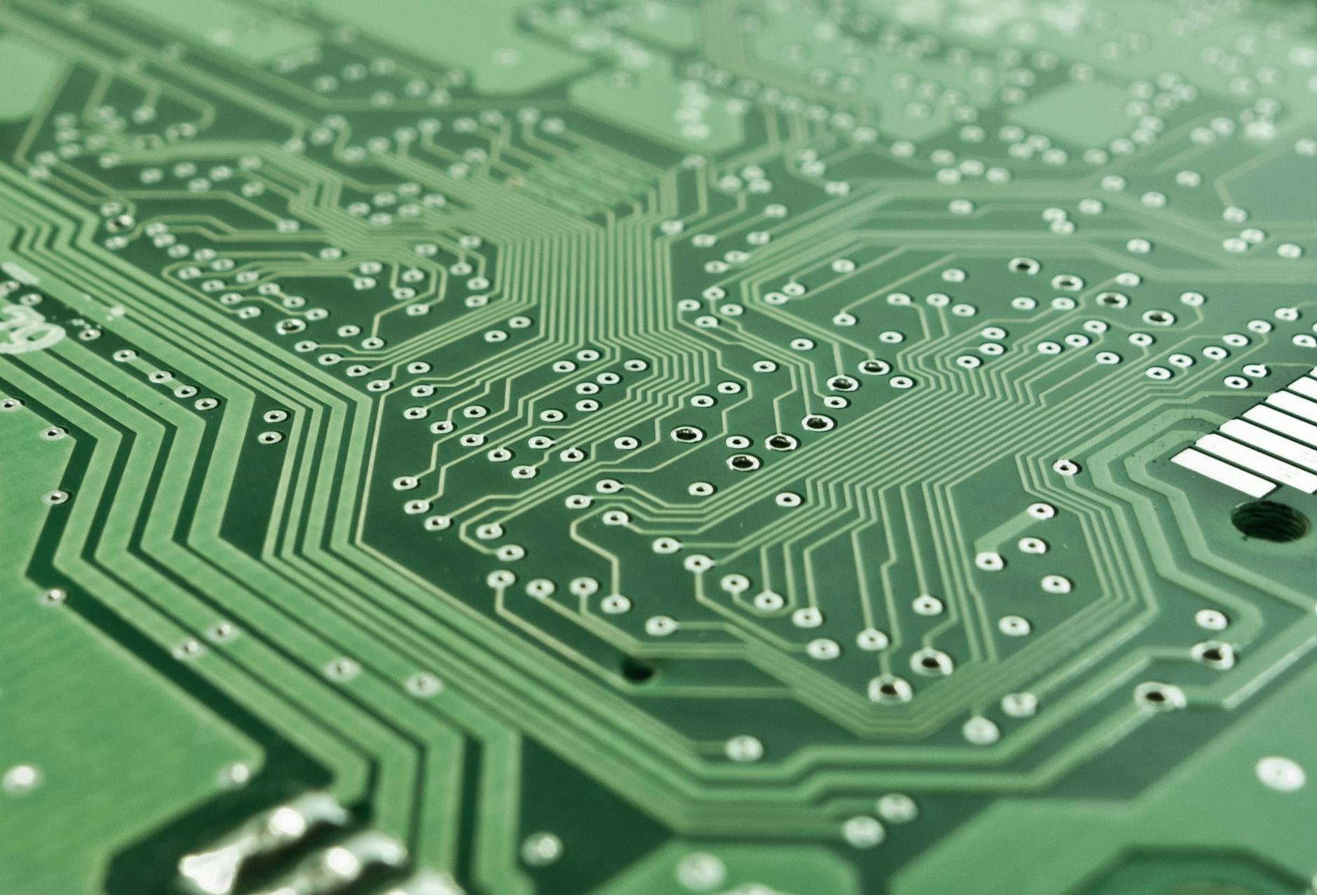
Huawei (华为) on Monday unveiled a new chip-architecture proposal it calls the Tau (τ) Scaling Law, a move that Beijing and some analysts say could accelerate China's push for semiconductor self-reliance and blunt the bite of US export controls. It has been reported that Huawei claims the law lays the groundwork to reach transistor densities equivalent to a 1.4‑nanometre process in high‑end chips by 2031 — a bold target that, if realised, would narrow the gap with global leaders in advanced node design.
What Huawei says — and what remains unproven
Huawei’s semiconductor executives reportedly argue the Tau law offers an architectural workaround that makes extreme ultraviolet (EUV) lithography equipment unnecessary to hit future node-equivalent densities. He Tingbo, chairwoman of the Huawei Scientist Committee, said cutting‑edge EUV tools would no longer be required. But these are technical claims that still need testing in silicon, in fabs and at scale. Reportedly promising in theory is not the same as shipping commercial, repeatable silicon.
Geopolitics and market stakes
The announcement lands squarely in the geopolitical contest over advanced chips. US-led sanctions have constrained China’s access to EUV tools and other high‑end manufacturing inputs, and Beijing has made self-sufficiency a strategic priority. “The US will have less leverage over export control as China becomes more self‑sufficient,” one economist told reporters, while also warning the approach remains to be proven. Who stands to lose most if the approach works? Nvidia — whose GPUs dominate AI training and inference markets — is widely viewed as the company that would be most threatened by a credible Chinese alternative to Western AI compute stacks.
If Huawei’s claims survive peer review, prototyping and yield ramp, the implications are large: a narrower technological divide would complicate US export policy and reshape supplier relationships across the semiconductor ecosystem. For now, however, analysts stress that the engineering, manufacturing and supply‑chain steps between a scaling law on paper and mass‑market AI chips are long and uncertain. Washington, Beijing and global markets will be watching the next practical tests closely.