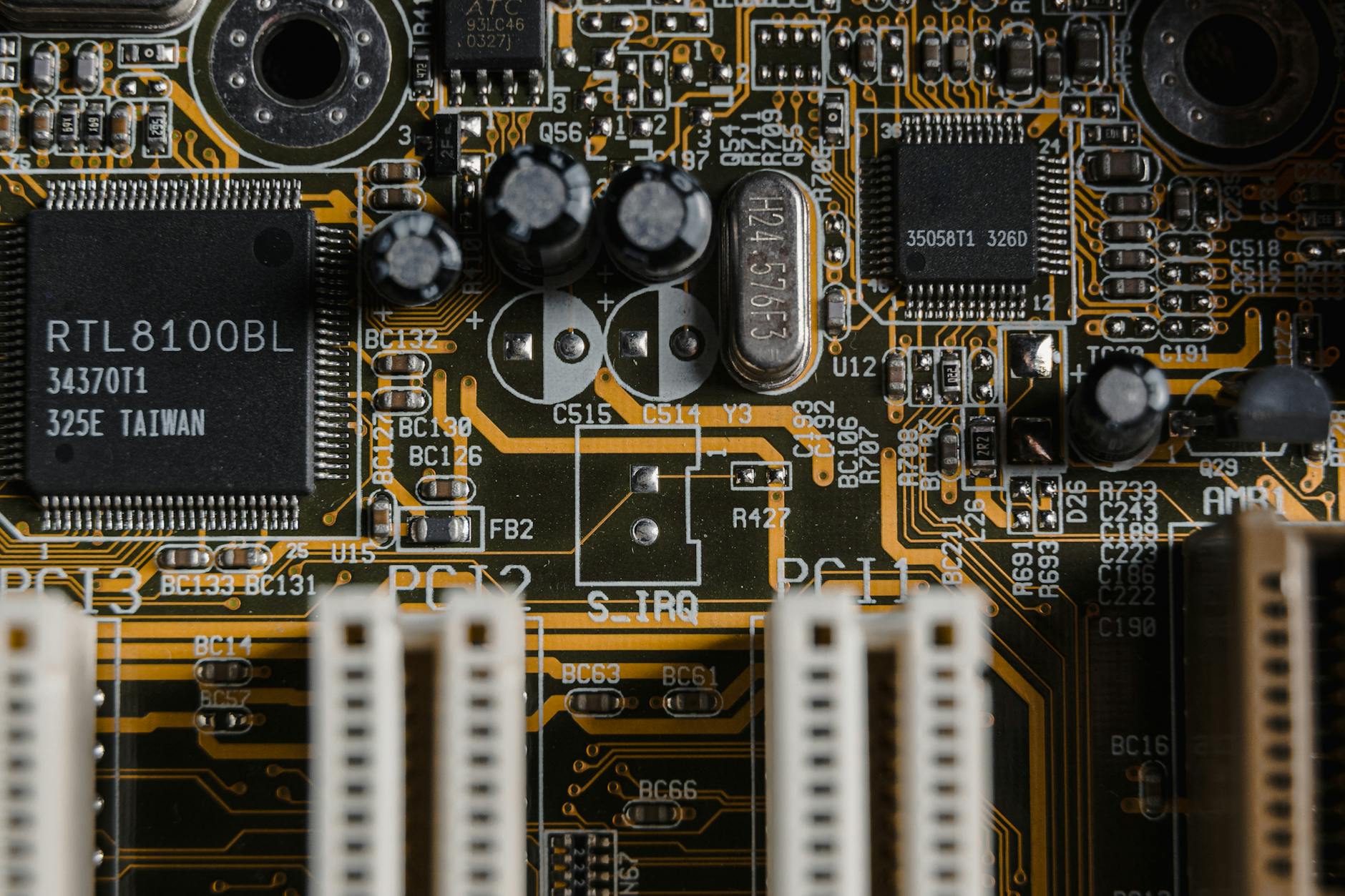
Huawei (华为) targets 1.4 nm for high-end chips by 2031 as "Tao's Law" is officially released
Ambitious roadmap unveiled
Huawei (华为) has reportedly set an ambitious internal roadmap aiming for a 1.4 nm-class process node for high-end chips by 2031, coinciding with the release of an internal guideline dubbed "Tao's Law." It has been reported that the guideline formalises multi-stage targets for process scaling, architecture innovation and ecosystem development — a signal that Huawei is publicly articulating a long-term, high-risk push back into leading-edge semiconductors.
Why this matters (and why it's hard)
For Western readers: reaching a 1.4 nm node would place Huawei at the bleeding edge of semiconductor physics, well beyond today's commercial nodes and requiring breakthroughs in lithography, materials and design. It is reportedly that Huawei's chip-design arm HiSilicon (海思) and related R&D units will drive the effort. But there are major practical barriers. Advanced extreme ultraviolet (EUV) lithography systems from suppliers such as ASML, specialised deposition and etch tools, and EDA software are tightly controlled by export regimes — a geopolitical constraint that has complicated China’s push for chip self-sufficiency.
Geopolitics and the domestic drive
The target must be read in the context of sanctions and trade policy. Since 2019–2020, U.S. export controls have restricted Huawei’s access to some U.S. technologies and to advanced chipmaking equipment. Those measures pushed Chinese firms and policymakers to accelerate domestic supply-chain development. Reportedly, "Tao's Law" is as much a technical plan as it is a strategic statement: an attempt to set expectations internally and to mobilise talent, capital and local suppliers for a decades-long campaign.
A long shot with big implications
Can Huawei overcome physics, tooling and ecosystem constraints in less than a decade? Skepticism is justified. Even optimistic timelines from established foundries take years to commercialise each shrink. Still, the announcement matters: it signals intent, prioritises resources and will likely spur further state and private investment across China’s semiconductor stack. Until concrete milestones are independently verifiable, however, readers should treat the 1.4 nm target as an aspirational beacon rather than a near-term certainty.