Huawei (华为) upends Moore’s Law with a “time-first” τ doctrine
What Huawei announced
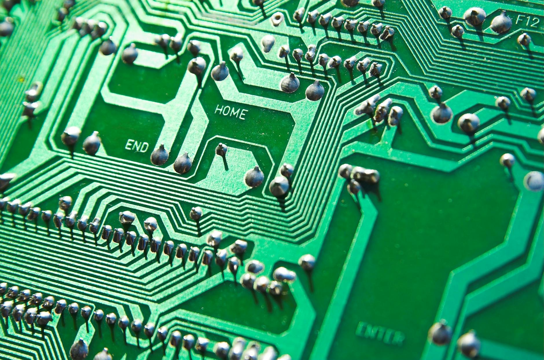
Huawei (华为) has formally proposed a new guiding principle for chip development that shifts the focus from geometric scaling to time — a "τ (tau) law" that prioritizes reducing signal delay rather than only shrinking transistors. It has been reported that He Tingbo, president of Huawei’s semiconductor business, unveiled the idea at the 2026 International Circuits and Systems Symposium, and that the company outlined a roadmap of techniques — logic folding, 3D integration, advanced packaging and software–hardware co‑design — to compress the circuit time constant τ and thereby boost system performance. It has also been reported that Huawei set an aspirational target of achieving "equivalent 1.4 nm performance density" by 2031; note the company used the word "equivalent."
Why this matters — technical and geopolitical context
Moore’s Law historically meant making transistors smaller to raise performance and lower cost. But as physical limits bite and EUV‑class equipment remains tightly controlled, that path has become ever costlier and geopolitically fraught. For Western readers: China’s access to the most advanced process tools has been constrained by export controls and sanctions, so alternatives that deliver system‑level gains on mature nodes have real strategic appeal. τ‑law reframes the problem: instead of asking "who can make the smallest transistor?" the question becomes "who can make signals run fastest across a stacked, heterogeneous system?"
Market reaction and likely winners
Equity markets reacted sharply. It has been reported that foundry and packaging names jumped in afternoon trade, with Hua Hong Semiconductor (华虹半导体), SMIC — Semiconductor Manufacturing International Corporation (中芯国际), JCET Group (长电科技), Tongfu Microelectronics (通富微电) and Huatian Technology (华天科技) among the movers, and the Sci‑Tech Innovation 50 index hitting new highs. The deeper industry implication is that value may migrate away from a single‑minded node narrative toward companies that can deliver system integration: advanced packaging houses, EDA and simulation firms, and specialized test, materials and equipment suppliers. Empyrean (华大九天) for EDA, NAURA (北方华创) and AMEC (中微公司) for equipment, and materials and test suppliers such as Anji Technology (安集科技) and Jingce Electronic (精测电子) were all highlighted as having strategic roles to play.
Bottom line
This is not a repudiation of advanced process technology — extreme lithography and device innovation remain important — but a strategic reorientation that could let Chinese firms "change lanes and overtake" by optimizing system‑level latency and integration rather than chasing node labels alone. Investors should ask which players can prove technical capability, secure customer validation and deliver volume; rhetoric and a headline "1.4 nm" number are not the same as manufacturable, validated performance.